As demand of OLED touch screen grows, electronics manufactures are increasingly turning to UV LED solution providers. Because UV LED has many advantages in the field of OLED flat manufacturing. The benefits to manufacturers have reliable solution including high productivity, environmental safety, friendliness, and how these products can be cured.
One of the most exciting features of OLED display is, they are more flexible, which is the important point for flexible / collapsible display device. In the near future, It will be a compelling feature for clients and industries. The encapsulation layer of a curing OLED display is essential to prevent damage to elements in its life cycle.
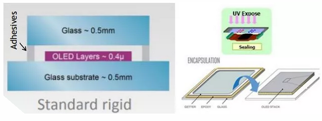
However, the actual OLED material is easily oxidized by very small amounts of water and oxygen in the atmosphere. Therefore, it is very important for a barrier or seal protect sensitive OLED materials from oxygen and water. The encapsulation of traditional rigid glass substrate is used cover glass. The cover glass must be permanently glued to the glass substrate to protect the effective OLED layer. The is achieved by applying a layer of epoxy resin on the edge of the glass and using UV LED lights to solidify the epoxy resin and the edges of the two glass surfaces.
 |
| https://www.leduvcuring.com/ |
In order to make the display more flexible, glass plate at the bottom and top are replaced by flexible substrates. Flexible thin-film encapsulation (TFE) is necessary. The barrier layer thickness is usually located within he sub-micro range to meet the low permeability requirements of WVTR < 10-6g / m2 / day. But it still flexible. TFE is consisted with alternating conformal organic and inorganic layers to achieve low permeability and high elasticity. When the thin inorganic layer as a barrier layer, the organic layer is utilized as the “decoupling” layer between the inorganic layers to improve penetration. What’s more, as a single inorganic layer in the organic / inorganic multilayer structure can kept thin. The organic layer makes the structure stronger and more flexible. The whole structure is also more resistant to fragmentation and cracking, when the organic layer as a seal buffer to smooth the substrate.
 |
| https://www.leduvcuring.com/ |
TFE manufacturing Techniques including :
1.Vitex vacuum polymer
2.Inject printing (organic), sputtering (inorganic)
3.Plasma enhanced chemical vapor deposition (PECVD) / atomic layer deposition (ALD)
Vitex process generates a flexible encapsulation layer composed of AI203 and polyacrylate layer. When the inorganic AI203 is sputtered to the display by plasma, UV curing to deposit organic polyacrylate layer by flash monomer, repeat the alternating process to form a multilayer structure.
Although this UV encapsulation solution exhibits excellent performance for flexible devices, the complexity raises many challenges to the manufacturing process.
 |
| https://www.leduvcuring.com/ |
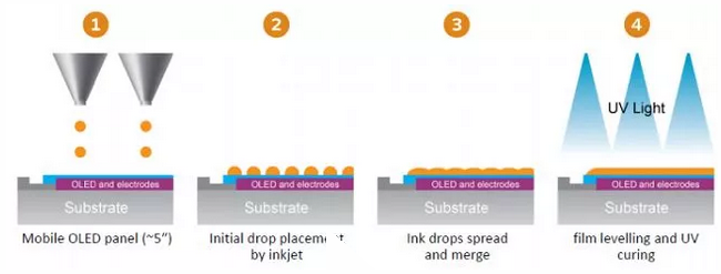
The OLED encapsulation based on inkjet printing is starting to replace OLED encapsulation based on chemical vapor deposition (CVD) in process optimization and precision, leading to better performance and productivity. It is said that the TFE organic sandwich of inkjet printing has a very high uniformity, eliminating the uneven display of the eye (“mura”). In addition, due to printing and post-printing processing in very low H2O and O2 environments, fewer particles are added by the printing process, and the plane of the organic layer at the top is significantly improved to ensure the quality of the second inorganic layer.
After applying the liquid organic layer through the inkjet nozzle, the UV curing step is performed to form the crosslinking.
 |
| https://www.leduvcuring.com/ |
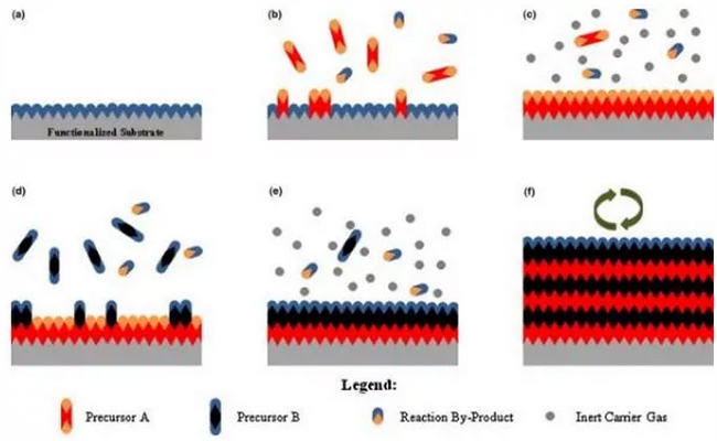
ALD process has been developed to produce a very thin conformal film with thickness control. This is a continuous self-terminating CVD process that can be coated with high quality. It is usually made up of alternating pulses with a gaseous chemical precursor that reacts with the substrate. During each gas surface reaction (half reaction), the amount of time specified by the precursors in the vacuum pulsed into the chamber is allowed to be fully reacted with the substrate surface. Then the inert gas purge chamber is used to remove any unreacted precursor or reaction byproduct. The process loops until the appropriate film thickness is reached.
ALD process has many promising features, but the deposition rate is slow. UV LED is not required in this process.
 |
| If you has any question, please send to 1651063690jennifer@gmail.com |
No comments:
Post a Comment