DSX-KYUV30 Low Temperature UV Masking Instant Super Curing Glue Semiautomatic UV LED Exposure Machine
The exposure and masking system, is the first UV LED masking system available on the international market. The UV LED masking system is a compact exposure-masking system equipped with an LED based optical head, collimated and homogeneous.
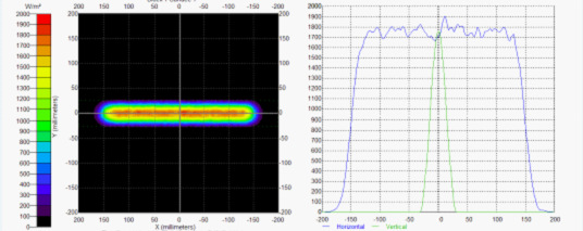
Its masking function enables to reach resolutions less than 2µm. It’s a new approach of masking, LED generation, unrivalled collimation performance.
Features of DSX-KYUV30 UV LED Masking System :
1.Zero maintenance cost. It does not need to replace the light source parts for long-term work.
2.Long life design. It can continue to work 20000 hours.
3.Low irradiation temperature
4.Single band UV
5.No harm to human radiation light
6.Touch screen display interface, parameter modification, automatic data saving, simple and reliable operation.
7.The built-in cooling system ensures long-term normal operation.
8.With light intensity correction control circuit, ensure the uniformity of light.
9.Bottom up irradiation, convenient for wafer placement.
Parameters of Best UV LED Exposure System for photolithography :
Outside Dimension
|
584 L*540W*184H mm
|
Input Power
|
AC 110V – AC 220V
|
UV Wavelength
|
365nm (385nm selectable)
|
Irradiation Direction
|
Bottom up irradiation
|
Parameters Setting
|
Touch-Screen Operation
|
Suitable for Wafer Size
|
6”,8”,10”, 12”
|
Tips for Finishing UV Masking
|
Buzzer Alert (or set automatic exit)
|
Time for Finishing
|
Based on UV tape characteristics (can be as short as 20s)
|
Time Settings
|
Unlimited, the smallest unit is 0.1s
|
Exposure Settings
|
20%~100%, with its own light intensity correction circuit, the irradiation intensity is constant.
|
System Fittings
|
Can be customized
|
How the Photolithography System Works
The Photolithography System works by exposing the photoresist layer on the plate to intense monochromatic UV light. This uniform, 365nm UV light is emmitted by the machine downward in a nearly parallel direction. A patterned masking slide is placed over the plate. This blocks the UV light from reaching the photoresist layer in the desired pattern. In our case, since we are using positive photoresist, the exposure to the UV light degrades the still exposed photoresist layer and allows it to be removed by the developer in a later step.
Introduction of Best Wafer UV Exposure :
The UV Exposure and Masking System is to use UV LED cold light source. Wafer UV Exposure Machine provides the standard 365nm UV. At the same time, according to user requirements, the wafer UV exposure machine provides 385nm, 395nm and 405nm UV light source, is suitable for optical, biological technology, microelectronics, wafer bonding, curing, a variety of applications, such as cell culture, is widely used in UV Exposure.
This set of UV LED Exposure adopts the leading LED light source technology, fully realizes the single wavelength UV cold light source illumination, effectively eliminates the thermal effect, and is very suitable for the use of ultraviolet exposure in the laboratory or ultra-clean room.
Wafer UV Exposure System is compact in structure, easy to move, using touch screen control operation, completely effective and safe control of UV Masking room.
LED UV Light Source of UV Mask Exposure Machine has a service life of up to 10,000 hours, which is very reliable and durable, does not need daily maintenance, and is very convenient to use.

No comments:
Post a Comment